Loading…
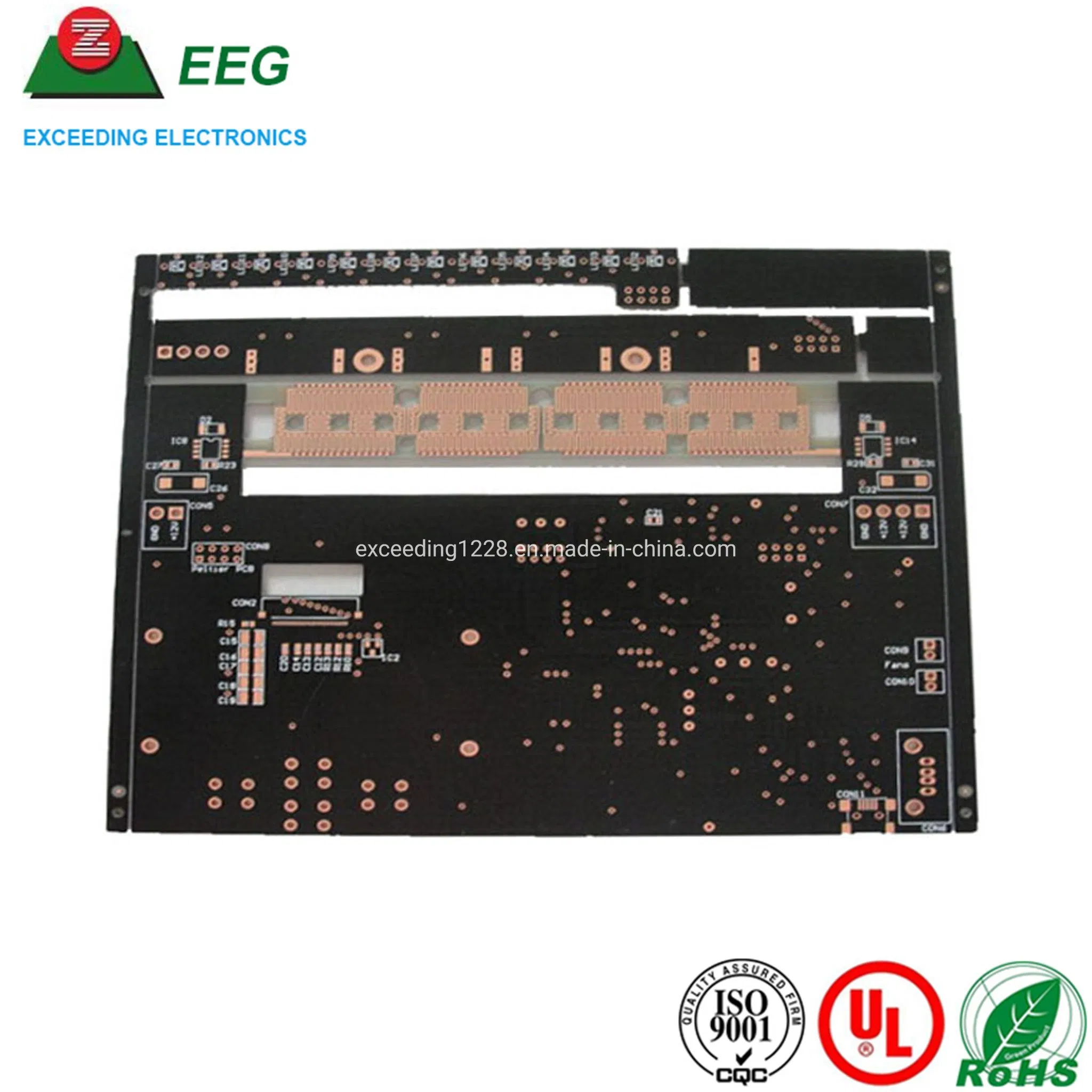
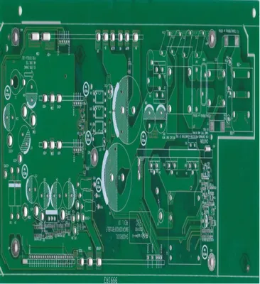
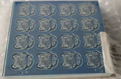
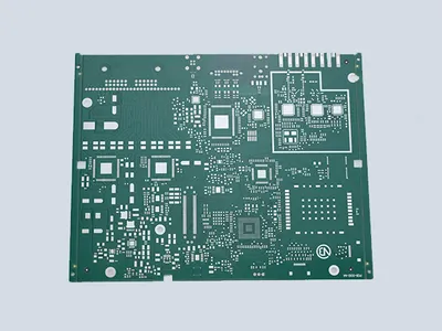
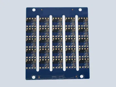
Advanced HDI Circuit Board Electronic PCB with Blind and Buried Vias
5.0InStock Source-listed auditby EXCEEDING ELECTRONICS GROUP LIMITED
₹8≈ $0.1 · indicative, confirm with supplier
Payment
T/T, PayPal, Western Union, Small-amount payment, VTB
Incoterms
FOB, CFR, CIF, DDP, DAP, EXW
Description
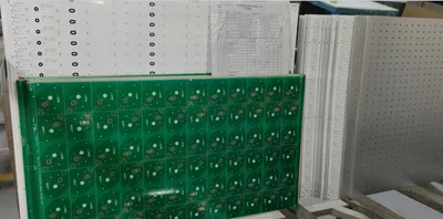
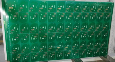
Advanced HDI Circuit Board Electronic PCB with Blind and Buried Vias. Advanced HDI Technology: Features blind/buried vias, sequential lamination, and solid copper filled micro vias. Heavy Copper Capability: Supports heavy-copper up to 12oz for high current applications. Large Board Dimensions: Maximum board thickness up to 6.5mm and size up to 1010x610mm. Via in Pad Technology: Provides conductive and non-conductive filled vias for compact designs. Strict Quality Standards: Manufactured to UL and IPC standards using laser drills and LDIs. Diverse Material Options: Processes FR4, Rogers, Isola, Arlon, ceramics, and Alu/Copper base materials. Fast Delivery Service: PCB build time as fast as 2-3 days with 12-hour express options.
Specifications
TypeRigid Circuit Board
MaterialFiberglass Epoxy
Model NO.PE2237632
DielectricFR-4
CustomizationAvailable